


Intel was once the world’s largest semiconductor company, but its market cap plummeted in recent years as the chipmaker fell behind Taiwan Semiconductor Manufacturing Co. and spent billions of dollars trying to catch up.
Now, Intel has entered high-volume production of 18A, the new chip node it says will turn things around.
The biggest problem? Convincing a big chipmaker to trust Intel with manufacturing on the new node. For now, Intel’s only major customer is itself. The company’s long-awaited Core Ultra series 3 PC processor, code-named Panther Lake, will come to PCs in January as the first major product made on 18A.
“It’s become an internal node for now,” said Daniel Newman, CEO of Futurum Group. “So many companies have made such massive investments into TSMC to ensure yield, to ensure capacity wafers that they just will not make the switch just yet.”
Intel is pinning its hopes of attracting customers on a new chip fabrication plant, Fab52, in Chandler, Arizona, where CNBC got an exclusive on-camera tour in November. Some 50 miles north, in Phoenix, TSMC also has a new fab, where it’s making chips with 4 nanometer technology. Its most advanced 2nm tech is currently only made in Taiwan.
Intel’s 18A is generally on par with TSMC’s 2nm node in some metrics such as transistor density. But as Intel works out the kinks after years of delays on previous nodes, some 18A wafers have had defects, making for a lower number of usable chips per wafer, typically referred to as yield.
“Yields are always an issue at the advanced node. This is not an uncommon problem,” said Harvard Business School professor David Yoffie, who served on Intel’s board from 1989 to 2018. He pointed to early yield issues with Nvidia‘s Blackwell GPUs at TSMC that were quickly fixed.
Intel’s renewed focus on foundry — manufacturing chips for outside clients — came when Pat Gelsinger took the helm as CEO in 2021. Gelsinger was pushed out last December and replaced by Lip-Bu Tan in March.
“Over the past several years, the company invested too much, too soon – without adequate demand,” Tan wrote in a memo in July.
Intel’s campus in Chandler, Arizona, now includes five chip fabrication plants, with Fab52 being the newest addition, shown here on November 17, 2025.
Tony Puyol
With Intel awaiting a big outside customer, the U.S. government stepped up in August, taking a 10% stake in the company with an $8.9 billion investment, primarily coming from grants promised under the CHIPS Act signed by President Joe Biden in 2022.
Days earlier, SoftBank invested $2 billion in Intel, followed by a $5 billion investment in September from Nvidia, which agreed to use some Intel technology but didn’t commit to using its foundry.
Here’s a look behind the curtain of Intel’s new chip factory where it hopes to find major foundry customers and, with them, redemption.
Fall of a giant
Founded in 1968 by Silicon Valley chip pioneers Robert Noyce and Gordon Moore and legendary investor Arthur Rock, Intel brought the world’s first commercially available microprocessor to market just three years later.
From the late 1970s through the early 2000s, Intel pumped out increasingly advanced process nodes at a rapid pace, leading to the term “Moore’s Law” — the doubling of components on a chip every couple years.
“The 1990s was a period of wonder and excitement at Intel,” Yoffie said. “We were the world’s largest semiconductor company, the world’s most profitable.”
But Intel largely missed the mobile revolution, famously turning down a deal to make Apple’s processors for the original iPhone. Then came a whiff in AI.
In 2024, Intel saw its worst year ever, losing about 60% of its value. The plunge came after two of its previous chip nodes, 10nm and 7nm, were delayed by several years. Analysts say the delays may have been triggered by an earlier choice to hold off on using ASML’s costly Extreme Ultraviolet Lithography machines.
“I think we lost the discipline of cycle time,” said client computing head Jim Johnson, who joined Intel more than 30 years ago. “Cycle time requires you to commit and deliver, and we started talking ourselves into, hey, we can have longer cycle times and try and lift more or do more.”
As it hustles to get back on track, Intel told CNBC there will be at least 15 EUV machines in Fab52.
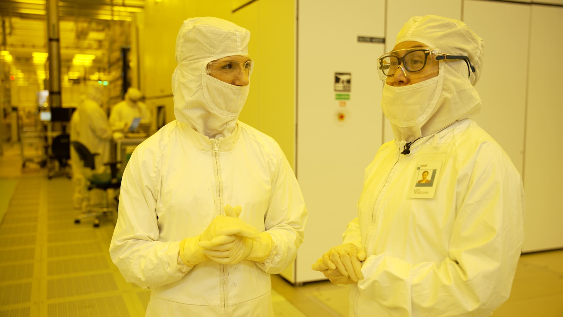
Intel 18A production manager Lea Tensuan shows CNBC’s Katie Tarasov the EUV machines inside Fab52 in Chandler, Arizona, on November 17, 2025.
By 2021, TSMC had become the node leader, and Intel began to outsource some leading-edge chip production to the Taiwanese giant. Around the same time, Apple began replacing Intel chips in Mac computers with its own M-series chips, also manufactured primarily at TSMC.
In his earlier stint at Intel, more than a decade before rejoining as CEO, Gelsinger “was given the responsibility to build a GPU to compete with Nvidia,” Yoffie said. “Unfortunately, that project failed and that ultimately meant we ended up not playing a significant role in the AI revolution.”
Intel may now be considering a deal to buy custom AI chip design startup SambaNova for $1.6 billion, though the company declined to comment on the matter.
‘Changing our culture’
The trademark of Gelsinger’s tenure as CEO was Intel’s focus on chip manufacturing. His ambitious roadmap had Intel catching back up to TSMC by releasing five nodes in four years.
Now, Tan is CEO and Naga Chandrasekaran is in charge of foundry.
“We are making yield improvements, defect density improvements, month-over-month and hitting our goals,” Chandrasekaran told CNBC in an interview in November. “So I believe we have turned the corner.”
Chandrasekaran joined Intel last year after more than two decades at leading memory maker Micron. He said his top goal is finding foundry customers.
“I have to become part of their team and convince them that they can trust Intel Foundry to execute,” Chandrasekaran said. “That’s number one. And to do that, we are changing our culture. We are bringing a huge execution focus internally into Intel Foundry.”
Chandrasekaran told CNBC that Fab52 is capable of more than 10,000 18A wafer starts per week. There’s more than a million square feet of manufacturing cleanroom space in Arizona, with five fabs all connected by 30 miles of overhead track moving wafers between them. A sixth fab, Fab62, is expected to be ready around 2028.
18A also uses RibbonFet, Intel’s gate-all-around architecture that improves power control by fully surrounding the transistor, unlike previous designs that only contact the top and sides. Chandrasekaran said 18A offers “more than 15% performance per watt improvement” over Intel 3.
Perhaps the biggest way Intel stands out is in advanced packaging, the assembly and connections of chips onto the final systems where they appear in real-world applications.
Intel engineer Shripad Gokhale shows CNBC’s Katie Tarasov its next Xeon data center chip in Intel’s advanced packaging lab in Chandler, Arizona, on November 17, 2025.
Tony Puyol
CNBC went to Intel’s advanced packaging lab in Chandler to see several steps in the process, such as protecting chips with a polymer-based seal, and exposing them to a liquid that detects any defects. Yoffie said Intel’s advanced packaging “can help mitigate some of the power consumption problems.”
“One of the biggest problems today for everybody making chips for data centers is the power that it consumes,” Yoffie said.
Chandrasekaran said the Arizona fab is on almost 100% renewable energy. As for water, Intel’s Arizona facilities used more than 3 billion gallons in 2024 and returned 2.4 billion gallons to the local supply through a water recycling plant it has on site.
‘No blank checks’
Tan’s message to employees when it comes to spending on future foundry nodes is clear: “No more blank checks.” The company needs customers.
Intel’s big new Ohio chip fab is delayed until at least 2030, and Tan has made major cost cuts by slashing 15% of the workforce in July and axing projects in Germany and Poland.
“That’s what the company needed,” said Newman of Futurum. “It needed to be faster. It needed to be leaner. It needed to be more focused. It needed someone that would be a little bit more shrewd.”
Tan is waiting to see how demand shapes up before giving solid details about Intel’s next node, 14A. Chandrasekaran told CNBC it will first be developed in Oregon, with a goal of volume production in 2028.
Finding customers for 18A won’t be easy. Unlike TSMC which only makes chips for outside clients, Intel also makes devices powered by its chips, positioning it as a competitor to some of the customers it hopes to land.
“If I’m an Nvidia or AMD or Qualcomm or Broadcom, do you really want to put your secret sauce into a manufacturing operation where you’re giving Intel access to that secret sauce?” Yoffie said.
He suggests breaking out foundry into a different company.
“If you actually separated the two, I think you’d give Intel a much better shot at being successful,” Yoffie said. “And you’d also give the United States a much stronger position for being the home of a major semiconductor manufacturing organization.”
Intel client computing head Jim Johnson gives CNBC’s Katie Tarasov an early look at its Panther Lake CPU in Santa Clara, California, on November 12, 2025.
Marc Ganley
For now, Intel hopes Panther Lake will be a big proof point when it debuts in PCs from major companies like Samsung, Dell, HP, Lenovo, Asus and Acer in January. Intel’s next data center chip, Xeon 6+, is also made on 18A.
“If you’re a major company that wants to bet on a process node, you’re going to feel a lot more comfortable if you see Intel ramping the heart of their client product line to high volume on that process node,” Johnson said.
Microsoft and Amazon signed early deals last year committing to use Intel’s foundry for some of their in-house custom chips.
“It’s a good sign, but of course their volumes are very small relative to Nvidia and the other major chip companies,” Yoffie said.
Recent reports suggest AMD is considering manufacturing at Intel, and one analyst predicts Apple may once again make some Mac chips at Intel by 2027.
In the meantime, Intel got a lifeline with the U.S. government’s 10% stake.
“It shows the confidence that the U.S. government has in Intel and the belief that we need to have leading edge R&D and manufacturing on U.S. soil,” Chandrasekaran said.
The government investment came days after President Donald Trump called for Tan to resign, then reversed course.
“I worry sometimes about the scope creep here and how the U.S. could decide to take stakes in all kinds of things,” Newman said. “But you have industries that we have let leave the U.S. to an extent that put us into indefensible risk, and we need to bring them back.”
Some 92% of the world’s most advanced chips are made in Taiwan, following a decades-long decline in the percentage of chips made in the U.S.
“The stakes are incredibly high for Intel, for the U.S. and for the world,” Yoffie said. “The whole idea that the world’s most advanced products are dependent on a single location in an island a few miles off the Chinese coast is a terrible situation for the whole world to have to deal with.”
Chandrasekaran, for his part, is committed to turning Intel into a manufacturer of advanced chips.
“As a semiconductor community, we have to enable this solution for the world to move forward with AI,” he said. “There’s no other option than to be successful.”
WATCH: Inside the Arizona chip fab key to Intel’s redemption
https://www.cnbc.com/2025/12/19/intel-aims-to-find-clients-and-catch-tsmc-with-new-chip-fab-in-arizona.html


